Metamaterials | Circuit Metamaterials
Creating Artificial Response with Metamaterials
We often think of materials as being continuous throughout their volume, with unique, intrinsic properties that do not vary greatly from point to point. Ultimately, however, materials actually derive their properties from collections of discrete atoms, each too small for us to perceive with our eyes, and thus we are left with the illusion of matter being a continuous substance. Since we cannot perceive the constituent atoms that compose a material, we can only infer the properties of the atoms through the apparent properties of the material.
When we think about the interaction of a material with an electromagnetic wave, describing the motion of each individual atom to the wave is not only intractable, but is also unnecessary. Instead, we can imagine averaging over those individual responses, replacing the collection of atoms by a hypothetical, continuous material with effective material properties, in the same way that we perceive materials with our senses. These effective material properties—dictated by the properties of the individual atoms, as well as their mutual interactions—provide all of the information necessary to predict the behavior of waves whose fields vary on a spatial scale much larger than the constituent atoms or their interatomic distances. Because what we identify as a material has been historically based on what our eyes can resolve, we often designate a microscopic scale and a macroscopic scale based on visible wavelengths. Since the wavelength of visible light is roughly on the order of a half-micron, or 500 nanometers, atoms and molecules (being on the nanometer scale) are clearly in the microscopic scale. The macroscopic scale, then, would be on the order of a micron or greater.
The fundamental equations of nature that govern electromagnetic wave propagation, Maxwell’s equations, do not possess any preferential scale. The descriptions of microscopic and macroscopic, then, can be generalized to a wave of any wavelength that interacts with any collection of objects. For example, an aluminum soda can is an “atom” for all practical purposes for waves at radio frequencies, since the wavelengths for those waves can be hundreds of meters. If we arrange a bunch of soda cans into an array, we have created an artificial material for radio waves. The cans and their arrangement would be considered the microscopic description, while some set of effective medium properties would constitute the macroscopic description—in other words, the wavelength of visible light no longer sets the scale for what we consider microscopic or macroscopic.
So, now we can address the important question: “What is a metamaterial?”
The answer, given our discussion above, is: “Just about anything.”
That answer might seem unsatisfying at first, but it also holds the key as to why the metamaterial concept is so powerful. Metamaterials allow complete freedom for designing material properties; the only constraints are set by the fundamental laws of physics. With metamaterials, we can access the full range of material properties that Nature allows, and control those properties with unprecedented precision. This remarkable level of control has led to the demonstration of new materials, such as negative index materials, hyperbolic materials, zero index materials, or the transformation optical materials that are used to make invisibility cloaks and other unique structures. There is no limit to the geometry or materials used to make the “microscopic” metamaterial elements; metamaterial designers can exercise their imaginations and creativity, choosing from endless design possibilities that will produce the desired effects. All that matters is that the metamaterial elements and their spacing be smaller than the wavelengths of operation.
Although the design space for metamaterials is infinitely large, there have been several classes of metamaterial elements that have become commonly used throughout many metamaterial demonstrations. Starting from one of these basic metamaterial designs, one can span an enormous range of material properties simply by making small adjustments to a few geometrical parameters. Moreover, by adjusting the overall scale of the element, the desired response can be set anywhere across the electromagnetic spectrum. Below we describe circuit metamaterial elements, which we have used extensively in our research for many years.
Metallic Metamaterials: MetaCircuits
When designing a metamaterial, a good material to start with is a conductor. In a conductor, charges are free to flow in response to electromagnetic fields, and can create a very large response to incident electric and magnetic fields. At low frequencies (for example, frequencies below a terahertz), conductors can be assembled into tiny circuits, which enable anyone with even a little bit of electrical engineering or circuits background to immediately understand how to form metamaterials with desired properties.
The basic idea of material response is illustrated in the figure below, where we imagine first a wire or piece of metal to which we apply an electric field $E_{app}$. The conductor is initially charge neutral, but because electrons are free to move in response to the applied field, the piece of metal becomes polarized, with negative charges being induced on one side and positive charges induced on the other. This charge distribution is known as an electric dipole, and produces a set of fields that flow from the induced positive charges to the induced negative charges, as shown. The strength of the dipole moment is a constant times the applied field, so that $p=\alpha_e E_{app}$. The constant $\alpha_e$ is known as the electric polarizability.
We can also obtain a magnetic response from a conductor, as long as the incident magnetic field fluctuates as a function of time. If we have some loop of wire, like the coil shown in the figure, then a time-varying current will be induced in the conductor in proportion to the magnetic field that passes through the loop. This circulating current gives rise to a responding magnetic field that, if the loop is small enough, behaves exactly like a magnetic dipole. The effective magnetic dipole moment is the current multiplied by the area of the loop, or $m=I A$, and the strength of the magnetic moment is proportional to the applied field, or $m=\alpha_m H_{app}$. Here, the constant of proportionality $\alpha_m$ is the magnetic polarizability.

As pictured above, the metamaterial elements are conducting volumetric shapes, either something like the ellipsoid on the left or the coil of wire on the right. To form an artificial material, such elements would need to be constructed and then arranged into a volume, held rigidly in place by some means. While that approach to forming a metamaterial is certainly possibly, it is more convenient if planar fabrication can be used. A common and very inexpensive technique for creating metal patterns is UV (ultraviolet) lithography, often used to pattern microcircuits on printed circuit boards (PCBs) found in computers and other electronic devices. The same processes used for to produce PCBs can be easily modified to make metamaterials. The first metamaterials demonstrated, in fact, were fabricated using PCB lithography, which remains the dominant approach even today.
For many reasons, then, we refer to metamaterials produced by PCB technology and that rely on conductors for their primary response as circuit metamaterials. Especially at low frequencies (for example microwave or millimeter wave), circuit metamaterial designs can cover an astonishing range of material parameter space, enabling new material paradigms to be realized. In the following, we summarize some of the common circuit material designs used in our group and many other groups over the years.
Artificial Dielectrics - When a static electric field is applied to a piece of metal, positive and negative charges ($+Q$ and $-Q$) accumulate on the opposite surfaces and the metal becomes polarized as described above. If the conductor is fashioned into a strip of metal, as illustrated in the figure below, then the charges are separated a distance roughly the length of the strip, or $l$, and the dipole moment then (by definition) is $p=l Q$.
The amount of charge that accumulates must be related to the self-capacitance of the structure $C$, which means we can apply the simple circuit model shown below that consists of a voltage source acting on a capacitor. If we assume that the conducting element will be part of a repeated lattice, with elements spaced by distance $d$, then the applied voltage is $V_0=E_{app} d$. The magnitude of the charge that is induced on either side of the element is found from basic circuit theory as $Q=C V_0=C E_{app} d$. In this case, the effective capacitor is not a traditional capacitor, like a set of parallel plates, but rather relates to the energy stored in the fringing fields that extend from one end of the metal to the other. Thus, the circuit model is applicable and can still be used to gain considerable intuition. (Later on, we can find metamaterial designs that better resemble traditional capacitors and make that connection clearer.) Since the polarization is proportional to the charge, then we can relate the induced polarization to the applied field using the above equations as $p=l d C E_{app}$.

Once we have the polarization for a single element, there are just a few steps to turning that into the electric permittivity of an assembly of similar elements. This process is known as effective medium theory or homogenization, which is a way of taking into account interactions among all of the elements. To keep things simple for now, we neglect interactions and just work with the basic equations to form some intuition.
The polarization of the single element is related to the applied field by the polarizability $\alpha_e$, or $p=\alpha_e E_{app}$. When we have a medium of dipoles, though, the usual process is to work with the dipole moment per unit volume, or the polarization $P=p/V$. In the case considered here, $V=d^3$. Then, $P=p/v=(\alpha_e/V) E_{app}=\chi_e E_{app}$, where we define the electric susceptibility $\chi_e$. Finally, we can define the electric permittivity as
\[\varepsilon_{eff}=1+\frac{l/d^2}C\]We then see that a conducting element is polarized in an applied field, and that a metamaterial formed of such elements will have a positive permittivity (or dielectric constant) that relates directly to the self-capacitance of the structure. Any change to the geometry will change that capacitance, and thus change the effective polarization and dielectric constant of the composite.
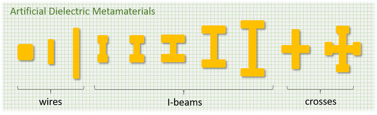
With the basic concepts in mind, we can see that if we want to increase the effective dielectric constant of an artificial medium, we need to increase the capacitance, and that means increasing the size or other characteristics of the region where charge can accumulate. In the figure below, we can see lots of different possible artificial dielectric designs that could be used for circuit metamaterials, including very simple wires, as well as “I-beam” structures that add sections to the top and bottom of the wire that bring up the capacitance. These structures will result in a medium that is anisotropic; that is, its properties will vary in different directions. Along the length of the wire, for example, there is a strong polarization and a composite medium will have a correspondingly large dielectric constant. Along the directions perpendicular to the wire axis, the response will be very weak. If we actually want a material that is more isotropic, we can consider the cross structures toward the right of the figure, in which we can control the dielectric constant in the two different directions by adjusting the lengths of the wires independently.
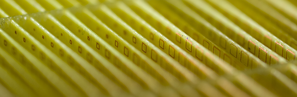
With the basic building blocks for artificial dielectrics in hand, there is no end to the types of structures that can be created. In our group, we have used artificial dielectrics to create a variety of quasi-optical structures that operate at microwave frequencies, as well as infrared and even visible frequencies. The example below shows a lens, made using I-beam elements and the familiar printed circuit board approach. As with many structures designed for microwaves, where the wavelengths are roughly on the order of centimeters, the metamaterial elements are patterned on circuit boards using standard optical lithography, and then the circuit boards are cut into strips and cross-pieces, giving the “wine crate” assembly as shown in the photograph. Because there is very little material actually required, these artificial dielectrics can be very lightweight and flexible.

Instead of modifying the surface of a material that has the same properties throughout its volume (that is, it is homogeneous), another way of controlling waves is to create a material whose properties vary throughout the volume (an inhomogeneous material). Gradient index lenses, frequently used in optics, are one example of inhomogeneous materials used to focus and steer light. Making inhomogeneous metamaterials is very easily accomplished, since the geometry of every element is determined during the design phase and is individually fabricated. The example below shows a close-up of a structure used to bend microwaves as they pass through the medium.
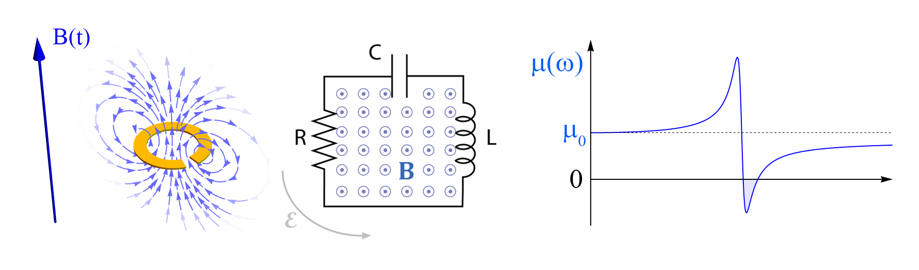
Artificial Magnetism - One of the more compelling aspects of metamaterials has been the ability to create artificial magnetism—magnetic response without the use of inherently magnetic materials. Because electromagnetic waves possess both electric and magnetic fields, obtaining complete control over these waves requires controlling both the electric permittivity, $\varepsilon$, as well as the magnetic permeability, $\mu$. Magnetic response in materials tends to occur at very low frequencies, and has all but vanished near visible wavelengths. Although suggested early on, artificial magnetic materials did not catch on until more recently in the context of metamaterials. Reintroduced by Sir John Pendry in 1999, the split-ring resonator, illustrated below, can act as a polarizable magnetic dipole, even though it consists primarily of conducting material (and no inherently magnetic components).
How is it possible to obtain a magnetic response from a conductor? The trick is to create a loop as shown in the illustration below. If one were to apply a constant magnetic field along the axis of the ring, nothing would happen; there would be no magnetic response. Only inherently magnetic materials can provide a magnetic response to static fields (with some particular exceptions). However, if the magnetic field varies as a function of time, then Lenz’s Law suggests that a circulating electric field (leading to an electromotive force) will be induced that can drive currents in the ring. Circulating currents are the essence of magnetism; once we have a responding current that flows in a loop, it will produce a responding magnetic field, as indicated in the figure.
Lenz’s Law provides the starting point to quantifying the magnetic response. The electromotive force induced around a loop is equal to the time rate of change of the magnetic flux density through the loop. If the loop has area $A$, then
\[EMF=-\frac{\partial \Phi}{\partial t}=-A\frac{\partial B}{\partial t}=-j \omega A B \]where we have assumed the incident field varies harmonically with time. The EMF acts like a voltage, so it is useful to model the ring as a little circuit. Any length of conductor will have an inductance $L$ and a resistance $R$. By opening a little gap in the ring, we also add some capacitance $C$, and the circuit becomes a series $RLC$ network. This model can easily be solved using basic circuit theory, and we find the responding current is
\[I=\frac{j \frac{\omega}{L}EMF}{\omega_0^2-\omega^2+j \gamma \omega}\]Here, $\omega_0^2=1/LC$ and $\gamma=R/L$. When a current flows in a loop, there is an associated magnetic moment which is simply $m=I A$. From this definition, we can determine the magnetic polarizability of the loop, $\alpha_m$. If we arrange the split-ring resonators into a lattice, as we did for the conducting rods in the example just above, then we can find an effective magnetic permeability for the structure, which has the form
\[\mu_{eff}(\omega)=\mu_0 (1+\frac{F \omega^2}{\omega_0^2-\omega^2+j \gamma \omega})\]All of the parameters in this final expression relate to the geometry of the split ring resonator, and thus the effective permeability can be designed at will by coming up with different resonator designs. A plot of the real part of the effective permeability shows the expected resonant form, and some important characteristics. First, at low frequency, $\mu_{eff}=\mu_0$, as expected. Since only inherent magnetic materials can provide a magnetic response to static fields, the magnetic effects in an artificial magnetic metamaterial must disappear. Second, the resonant circuit translates to a resonant magnetic response, which can have relatively large positive permeability, but also a region where the permeability is negative (shaded region in the figure above). This region of magnetic response was not so easy to achieve prior to metamaterials, and led to an explosion of creativity once it was demonstrated in the context of negative index materials. Also, as the frequency increases beyond the negative permeability region, there is a region where $0 < \mu_{eff}< 1$. This range of material parameters is also difficult to achieve with conventional materials, but has been extremely important in the realization of transformation optical media.
A sampling of the various metamaterial designs that have been demonstrated to date is illustrated below. In all of these cases, the overall size of the ring roughly sets the wavelength scale at which the structure will function. The total dimension of the ring should be smaller than the wavelength, usually significantly smaller. Starting with the approximate desired size, adding more capacitance lowers the resonance frequency, meaning that the region where the ring has its strongest magnetic effects shifts to longer wavelengths—something that is desirable for metamaterials. There are numerous ways to introduce more capacitance into the ring, including adding lumped capacitors strategically placed across gaps (not shown, but useful at very low frequencies), as well as creating dual ring (or multi-ring) designs. The final structure shown below consists of two parallel conducting segments or wires. This structure also behaves like a magnetic resonator, but can more easily be scaled towards the visible wavelengths.

Magnetic metamaterials have been used to create a wide range of novel and interesting structures and devices. The examples below are just a few that were constructed and measured in our lab over the years. The first sample shown below is composed of dual split ring resonators. The varying geometry for each resonator means there is a shift in the resonance of the effective permeability, so that this sample represents a disordered material. The next two samples are spiral designs, which introduce much more capacitance that they can strongly reduce the size of the element relative to the wavelength. The very dense spiral metamaterial elements in the third picture were designed to operate at around 12 MHz (~22 m wavelength), even though the element sizes were just about 2 cm—over a thousand times smaller than the wavelength. The final picture is of the original metamaterial “invisibility” cloak, which required a permeability that ranged between zero and one, just above the resonance in the figure above. This cloak had exacting parameters that required precise design and fabrication. Only a metamaterial could have provided the approach to realizing the transformation optical cloak.


Resonant Electric Materials - We’ve seen that conducting squares, short wires and other simple elements can be used to form artificial dielectrics—artificial materials that behave like insulating materials but with a controllable dielectric constant. The circuit model for these structures was simple: Just a capacitor. For the artificial magnetic structures, loops of wire are used to force current to circulate in a loop, behaving like little magnetic dipoles. Again, we could formulate a circuit model, which this time included inductance and resistance, in addition to capacitance. The result of adding inductance into the model meant the element would possess a resonance, producing not only regions of large effective permeability, but also regions of negative permeability.
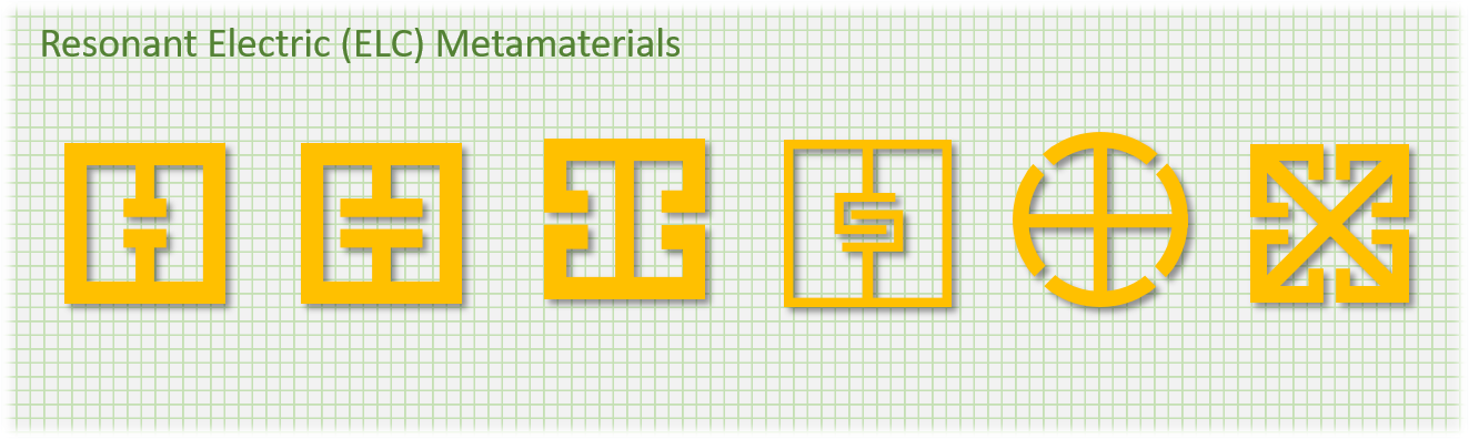
Having a resonant material response can be very useful for many reasons. So, the question naturally arises as to whether it is possible to create an electric metamaterial that will possess a resonant, effective electric permittivity in the same way that the split ring resonator possesses a resonant, magnetic permeability. The answer is to again create a resonant circuit, but in the way shown in the figure below. For the particular resonance of interest, currents will flow around the ring, but in the same direction as they charge the capacitor formed in the central region. Since there is no net current that circulates around the element, there is no magnetic response, and the resonance must correspond to an electric response.
Resonant electric metamaterial elements are sometimes abbreviated as ELCs, with the LC referring to the LC circuit resonance. There are two sources of capacitance in this case: The fringing fields like in the nonresonant wire shown in the first example above, with a capacitance $C_f$, and the capacitance in the gap, $C$. There may be other possible circuit models that can describe the ELC element, but the model shown captures some of the essentials. In particular, as the frequency approaches zero, the ELC has an electric polarization, just as the nonresonant, artificial dielectric. But at a higher frequency, there is a resonance where it is possible to achieve both regions of large, positive permittivity as well as regions of negative permittivity. The ELC, then, provides yet another crucial building block for metamaterials, and in many ways is the complement to the SRR. Near resonance, the effective permittivity is well-approximated by the expression
\[\varepsilon_{eff}(\omega)=\varepsilon_0 (1+\frac{\omega_p^2}{\omega_0^2-\omega^2+j \gamma \omega})\]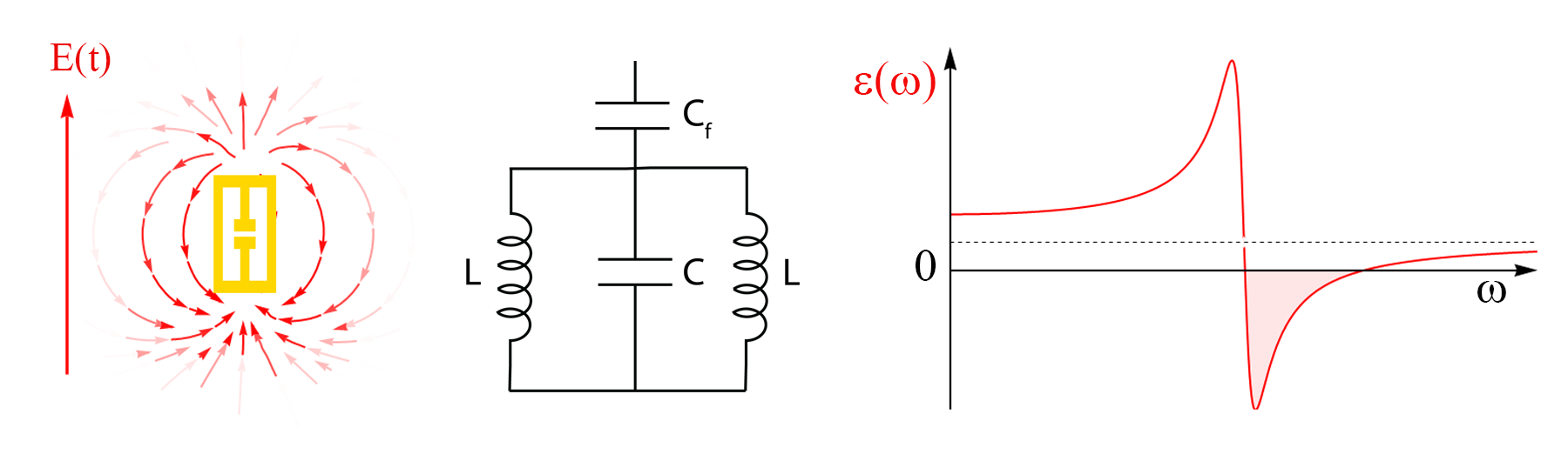
As is the case with artificial dielectrics and magnetic metamaterials, modifications to the size or geometry of the element changes the resonance properties, allowing the regions of large permittivity or negative permittivity to be placed anywhere in the electromagnetic spectrum. Though not quite as exotic as artificial magnetism, the ELC metamaterial is important because it enables precise control over the permittivity of a medium. The simple ELCs, consisting of a single capacitive gap between two inductive wires, can have many variations that allow for customized permittivity.
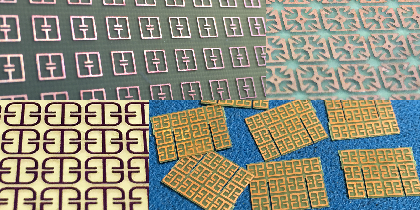
Below are several examples of ELCs from samples constructed in our lab for various microwave experiments over the years. These samples follow the same printed circuit board fabrication as described above, resulting in copper patterns on different types of dielectric PCBs. With these three types of elements—wires, SRRs and ELCs—it is possible in principle to create artificial materials with nearly any set of electromagnetic properties, limited only by the fundamental constraints imposed by the laws of physics. Conventional materials can only reach a subset of the electromagnetic properties that are theoretically available, and are not always easy to concoct with precision. Metamaterials, by contrast, can achieve a much wider range of properties, and those properties can be controlled point-by-point throughout the volume of the material.
Useful References
Magnetism from conductors and enhanced nonlinear phenomena
J. B. Pendry, A. J. Holden, D. J. Robbins, W. J. Stewart
IEEE Trans. Microwave Theory and Techniques 47, 2075 (1999)
Electric-field-coupled resonators for negative permittivity metamaterials
D. Schurig, J. J. Mock, D. R. Smith
Appl. Phys. Lett. 88, 081101 (2006)
A composite medium with simultaneously negative permeability and permittivity
D. R. Smith, W. J. Padilla, D. C. Vier, S. C. Nemat-Nasser, S. Schultz
Phys. Rev. Lett. 84, 4184 (2000)
Negative index materials composed of electric and magnetic resonators
R. Liu, A. Degiron, J. J. Mock, D. R. Smith
App. Phys. Lett. 90, 263504 (2007)